
Saturday, January 27, 2007
Intel's new 45nm fraud
Intel's bulk silicon is dead !
It is still fresh in our minds Intel's OFFICIAL fraud on 10-20 Ghz clocked processors, just around the corner, based on High-K and metal gates. This time, 10Ghz target is somehow dropped, but the other part of that fraud number one from past millenia remained.
Right, but what about the associated problems? 45nm itself alone is enough complex geometry to introduce sufficient number of production gremlins, even without High-K metal combination applied.
On the other side, Intel's some 40 years established bulk silicon production process is leaky enough to make Intel's standard SiO2 process ridiculous compared with AMD's SOI standards.
Intel did yet another fraud with 10Ghz. It REDUCED clock from former 3,8Ghz P4 to reduce power consumption and leakage in its dual cores. So, Intel masquaraded its max clock problem with NEW PROCESSOR ARCHITECTURE, that effectively replaced improvements that should be expected from its new 65nm process alone.
Though, 51 element is used in its production.
Now, Intel's marketing gun is empty and hard risky choice is ahead: To introduce radical new winning High-K metal process, or to suck AMD again in the next 2 years.
"It is claimed to increase transistor switching speed by 20%"
So, after "really big breakthrough" we will potentially get in the end shocking Intel's MAX 3,6 Ghz dual cores in 2009 !. In 45nm High-K.
"With 400M transistors"!
However, it is not stressed that Intel's 45nm core ITSELF has not necessarily more that 4M transistors !Why? Because the rest of chipbelongs to UNNECESSARY big cache, due to high IPC architecture, and and and ... LOW High-K process reproducibility. Consequently, that means in practice that new celebrated Intel's 45nm will be cheap and frequent like hen's teeth.
Intel first used the combination of metal gates and high-k dielectrics on the test SRAM (static RAM) chips it built using its 45-nanometer technology, Bohr said. The dielectric must be built using atomic-layer deposition, he said, meaning that a machine must deposit the dielectric just one atomic layer--the width of a single atom--at a time.
AMD will still remain cheaper, better and more competitive.
So in the end, where is essentially that Intel's breaktrough?
Nowhere.
Only yet another Intel's big lie.
And why 45nm fab is displaced to Kiryat Gat, Israel?
No one will be able to sniff the truth.
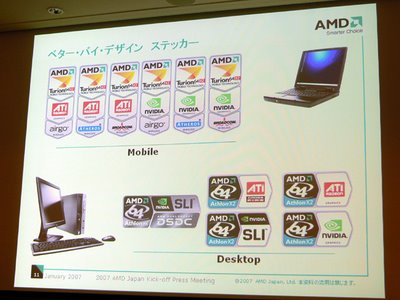
And the truth is against the Intel: AMD is smarter choice by design, not only in 2H2007.
AMD processor has on average 2 times less transistors than Intel's. QUite enough for the same productivity with older geometry, compared to Intel. So, what new technology means for AMD? Nothing. They only have to be compeatable with their older SOI production geometry (compared to Intel's bulk up to now). And that is just what they are doing now:
It is still fresh in our minds Intel's OFFICIAL fraud on 10-20 Ghz clocked processors, just around the corner, based on High-K and metal gates. This time, 10Ghz target is somehow dropped, but the other part of that fraud number one from past millenia remained.
Intel shows off next generation transistors
Now,"The implementation of high-k and metal materials marks the biggest change in transistor technology since the introduction of polysilicon gate transistors in the late 1960s," says Intel co-founder Gordon Moore.Right, but what about the associated problems? 45nm itself alone is enough complex geometry to introduce sufficient number of production gremlins, even without High-K metal combination applied.
On the other side, Intel's some 40 years established bulk silicon production process is leaky enough to make Intel's standard SiO2 process ridiculous compared with AMD's SOI standards.
Intel did yet another fraud with 10Ghz. It REDUCED clock from former 3,8Ghz P4 to reduce power consumption and leakage in its dual cores. So, Intel masquaraded its max clock problem with NEW PROCESSOR ARCHITECTURE, that effectively replaced improvements that should be expected from its new 65nm process alone.
Though, 51 element is used in its production.
Now, Intel's marketing gun is empty and hard risky choice is ahead: To introduce radical new winning High-K metal process, or to suck AMD again in the next 2 years.
"It is claimed to increase transistor switching speed by 20%"
So, after "really big breakthrough" we will potentially get in the end shocking Intel's MAX 3,6 Ghz dual cores in 2009 !. In 45nm High-K.
"With 400M transistors"!
However, it is not stressed that Intel's 45nm core ITSELF has not necessarily more that 4M transistors !Why? Because the rest of chipbelongs to UNNECESSARY big cache, due to high IPC architecture, and and and ... LOW High-K process reproducibility. Consequently, that means in practice that new celebrated Intel's 45nm will be cheap and frequent like hen's teeth.
Intel first used the combination of metal gates and high-k dielectrics on the test SRAM (static RAM) chips it built using its 45-nanometer technology, Bohr said. The dielectric must be built using atomic-layer deposition, he said, meaning that a machine must deposit the dielectric just one atomic layer--the width of a single atom--at a time.
AMD will still remain cheaper, better and more competitive.
So in the end, where is essentially that Intel's breaktrough?
Nowhere.
Only yet another Intel's big lie.
And why 45nm fab is displaced to Kiryat Gat, Israel?
No one will be able to sniff the truth.
And the truth is against the Intel: AMD is smarter choice by design, not only in 2H2007.
AMD processor has on average 2 times less transistors than Intel's. QUite enough for the same productivity with older geometry, compared to Intel. So, what new technology means for AMD? Nothing. They only have to be compeatable with their older SOI production geometry (compared to Intel's bulk up to now). And that is just what they are doing now:

THIS LINK posted by Joseph Bell : 8:57 AM

![]()


