Thursday, March 08, 2012

IBM drills holes into optical chip for terabit-per-second speed

Holey chip! IBM drills holes into optical chip for terabit-per-second speed
IBM researchers have built a prototype optical chip that can transfer a terabit of data per second, using an innovative design requiring 48 tiny holes drilled into a standard CMOS chip, facilitating the movement of light. Much faster and more power-efficient than today's optics, the so-called "Holey Optochip" technology could enhance the power of supercomputers. With the Holey Optochip, "our target is the bandwidth that interconnects different processors in the system—not the processor talking to its memory, but a processor talking to another processor in a large parallel system."
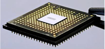
A single 90-nanometer IBM CMOS transceiver IC with 24 receiver and 24 transmitter circuits becomes a Holey Optochip with the fabrication of forty-eight through-silicon holes, or “optical vias” – one for each transmitter and receiver channel. The Holey Optochips are designed for direct coupling to a standard 48-channel multimode fiber array through an efficient microlens optical system that can be assembled with conventional high-volume packaging tools.
Talks are about the new 8.8Tbps (Terabit-per-second) national backbone network that Internet2 is building using Ciena's 100G coherent optical solution. Thus, one 1 Tbps opto chip is fast almost as the whole Internet2 backbone.

___________________________
99% BAD HARDWARE WEEK:

Comments: Post a Comment


<< Home

This page is powered by Blogger. Isn't yours?